Introduction
*General Description
*Architecture
*Hardware
*Front Panel Layout
*PCB Form Factor
*VME Connectors
*VME Interface
*VME Base Address
*Analogue Circuit
*Clock Sources
*Trigger Sources
*Resets
*Software
*Firmware
*Event Format
*Frame Finding
*Temperature Monitoring
*Power Block
*References
*The Front End Driver (FED) is a 9U 400mm VME64x card designed for reading out the CMS silicon tracker signals transmitted by the APV25 analogue pipeline ASICs. The signals are transmitted to each FED via 96 optical fibres at a total input rate corresponding to 3 GBytes/sec. The FED digitizes the signals and processes the data digitally by applying algorithms for pedestal and common mode noise subtraction. At high luminosity the input data rate is reduced using algorithms that search for clusters of hits. Only the cluster data along with trigger information of the event are transmitted to the CMS DAQ system using the SLINK-64 protocol. All data processing algorithms on the FED are executed in large on-board FPGAs.
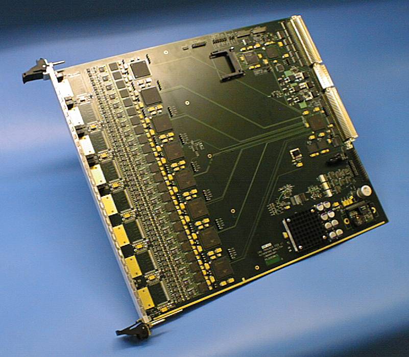
Figure 1 The FEDv1 board primary side.
Each FED receives analogue data from eight 12-fibre bundles corresponding to 192 APV25s. The FED front end comprises of 8 identical units each receiving and processing the data from 12 fibres. One front end unit consists of:
The variable length clustered data fragments from all 8 Front-End modules are collected on point to point links (4 bits @ 160 MHz) by a single "Back-End" FPGA (XC2V2000). This builds a FED event for each trigger from the data fragments and formats and stores them in an external memory buffer (2 MBytes deep) to cope with fluctuations in the data rate. The event buffer is implemented with a pair of Quad Data Rate SRAMs.
Finally the FED data are transmitted to CMS DAQ via 400 MByte/sec copper links using the S-LINK64 protocol implemented on standard DAQ mezzanine cards carried on VME transition boards. The same FED data buffer can alternatively be read via VME64x for test and monitoring purposes.
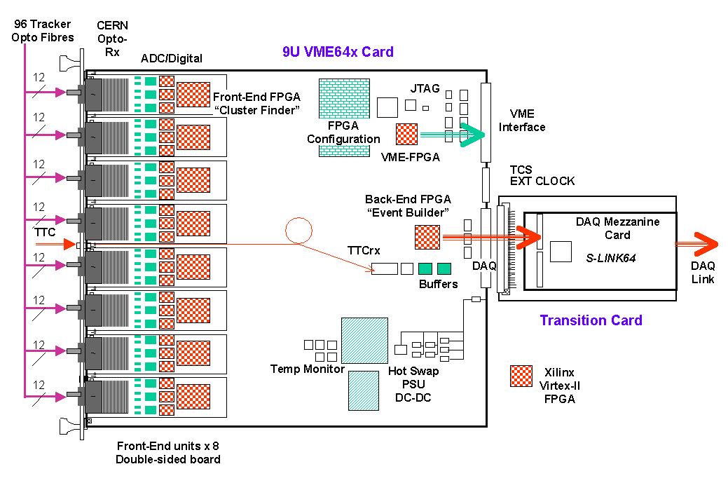
Figure 2 FEDv1 board layout with transition card.
Refer to Mechanical Drawing.
See also the LED description table.
VME 64x 9U x 400 mm (ANSI VITA 1.3-1997)
14 Layers (Signal/Gnd/Signal/Signal/Power/Signal/Power/Ground/Signal/Power/Signal/Ground/Signal)
Refer to Layers Drawings for details.
Standard VME64x : P1, P0 & P2 (ANSI VITA 1.1-1997)
For detailed Pin Descriptions refer to Schematics Sheet 11
FEDv1 is currently implemented as a simple D32 VME Slave. The FEDv1 board layout has all the necessary signal lines needed for full VME64x master and interrupt functionality if a future firmware upgrade is required.
Address Space : A32 Extended.
Size : 64 Kbytes.
Data Transfers : D32 ONLY (N.b. responses to D16/D8 accesses are undefined).
DMA : D32 transfers.
i.e. Following AM codes are permitted: 0F, 0E, 0D, 0B, 0A, 09
*FEDv1 does not provide arbiter functions and therefore each crate requires an arbiter card in Slot 1.
FEDv1 uses the Geographical Slot Address pins to fix its base address. It does not implement VME64x CSR dynamic addressing functionality.
A31 - A22 mapped to 0
A21 - A16 mapped to slot address
A15 - A1 mapped to FEDv1 space
Examples:
FEDv1 in slot 2 address range : $ 0002’0000 - $ 0002’ffff
FEDv1 in slot 21 address range : $ 0015’0000 - $ 0015’ffff
Jumpers
Refer to Assembly Drawings for details.
Clock Sources
FEDv1 can operate on 3 independent, exclusive clock sources selectable by software (see Figure 4) :

Figure 4: Clock Sources Block Diagram (click on picture for full size image)
Notes on clock changing:
FEDv1 logics can operate on 3 independent, exclusive trigger sources selectable by software :
A filter is applied which will only accept legal CMS trigger patterns i.e. single trigger pulse of width 25 nsec with no immediate neighbouring pulses.
Examples:
|
‘ 0000100000’ |
counts as 1 trigger |
|
‘ 0010010010’ |
counts as 3 triggers |
|
‘ 0011000000’ |
counts 0 triggers (calibration request to APV ignored by FED) |
|
‘ 0010100000’ |
counts 0 triggers (reset to APV) Resets FED BX counter. |
Refer to Software Pages.
Refer to Firmware Pages.
For detailed Pin Descriptions refer to Schematics Sheets 12,13 & 14.